|
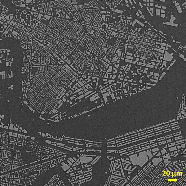
Map of Cambridge fabricated by focused ion beam milling and imaged by SEM. MIT’s infinite corridor is 25 µm long. |
|
|
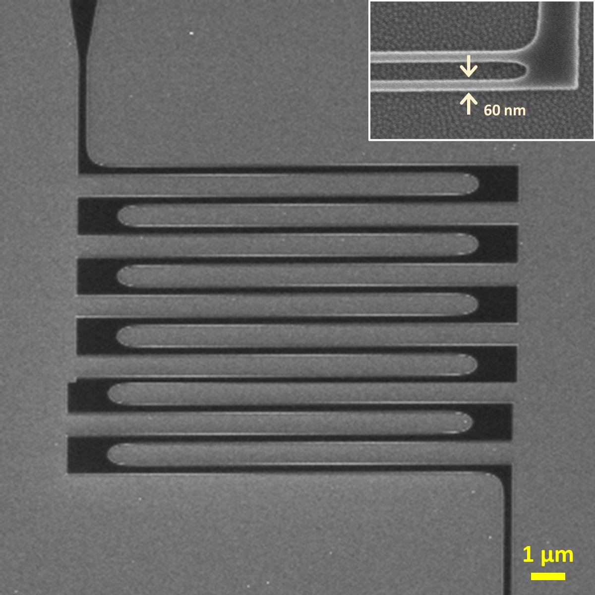
Superconducting nanowire single photon detector made from 4-nm-thick niobium nitride thin film on top of aluminum nitride substrate. The large meanders are integrated inductors to slow down the speed of the device. The narrow section of the nanowire (shown in inset), which consists of 60-nm-wide parallel wires, is extremely sensitive and able to respond to even single photons. Imaging was performed with Zeiss Sigma SEM. |
 |
|
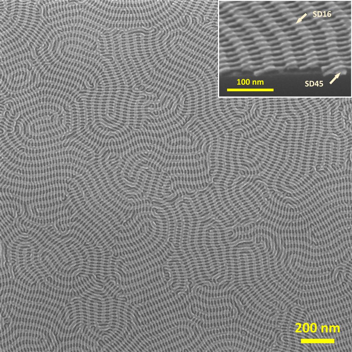
Oxidized PDMS cylinders from 16 kg/mol PS-b-PDMS (L0 = 19 nm) on top of oxidized PDMS cylinders from 45 kg/mol PS-b-PDMS (L0 = 43 nm) forming complex bilayer nanomesh structures. Background is silicon substrate. Imaging was performed with Zeiss Merlin SEM. |
 |
|
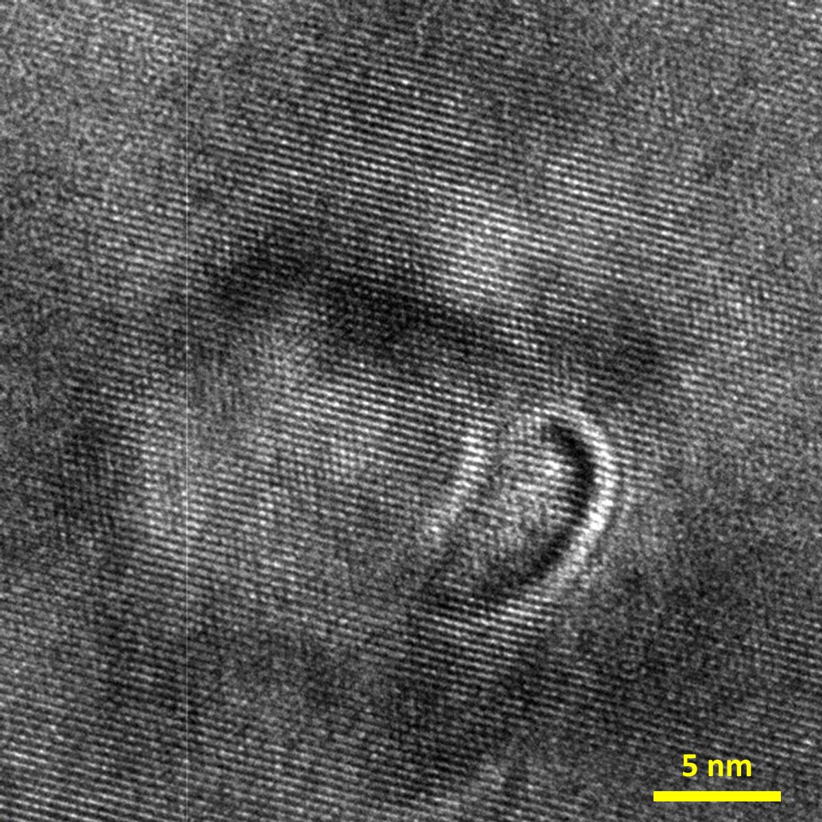
Rows of silicon atoms imaged by TEM. Beam damage at the center resulted in an ear-like shape. |
 |
|
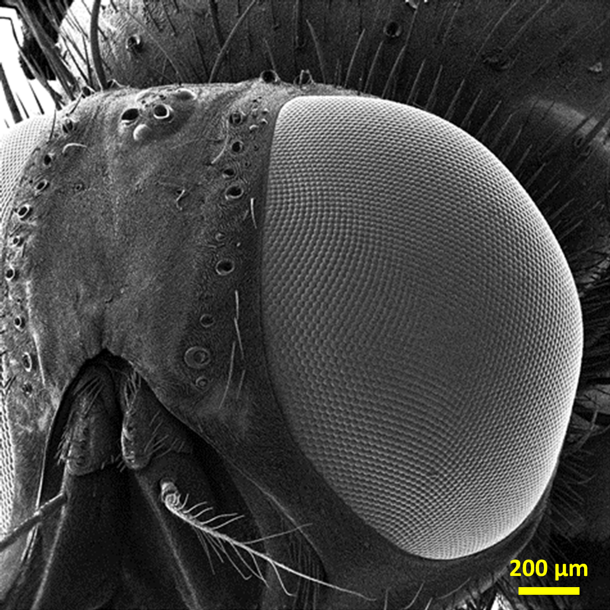
Fly imaged using Zeiss Orion helium ion microscope. |
 |
|
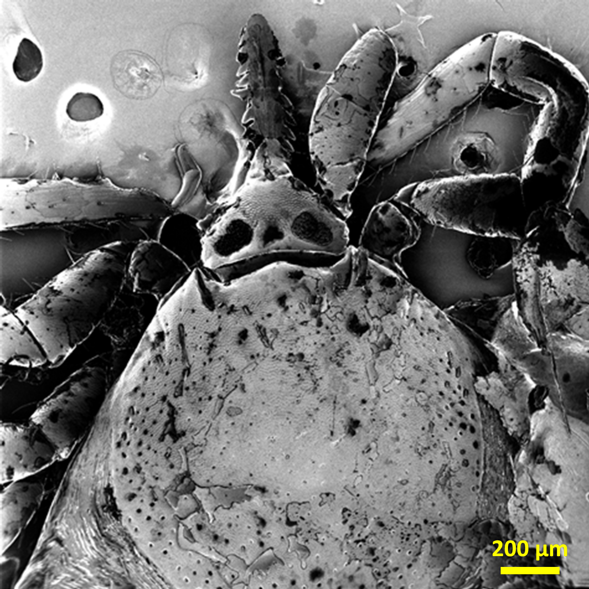
Tick imaged using Zeiss Orion helium ion microscope. |
 |
|
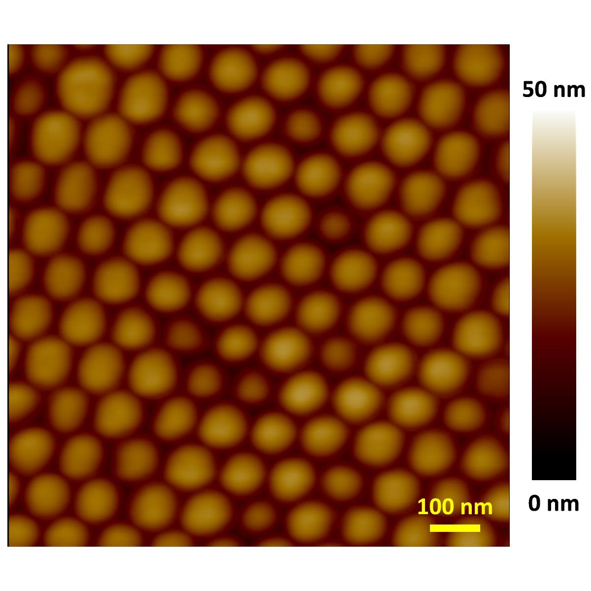
Surface topography of ion beam patterned cobalt nanomagnets imaged by AFM. |
 |
|
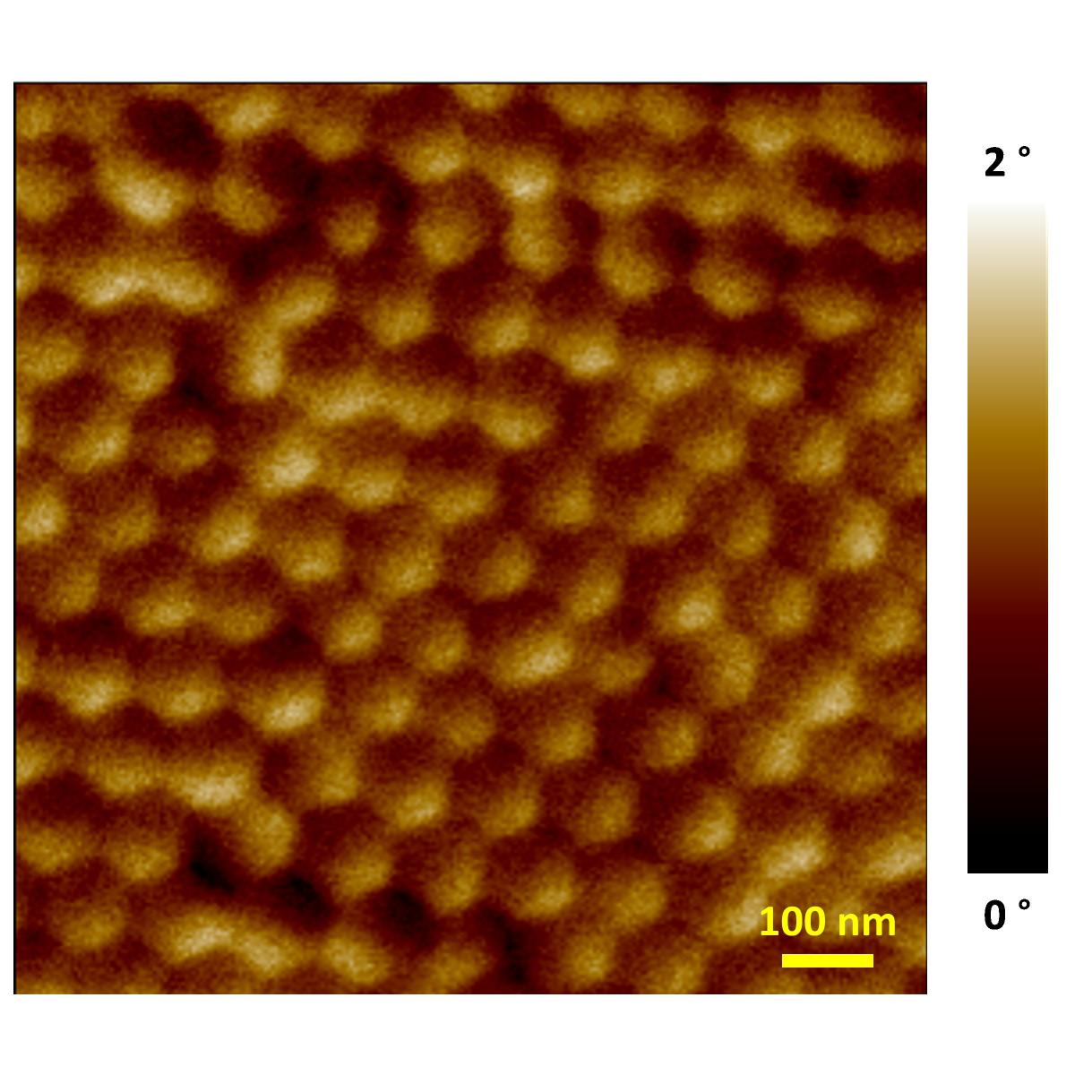
Magnetic response of ion beam patterned cobalt nanomagnets imaged by MFM. |
 |